
Pin out
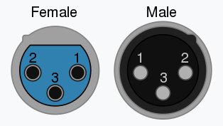
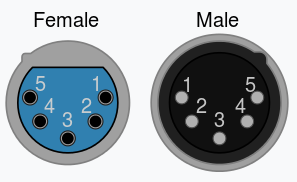
DMX pin out
- G -
Ground/Common- pin 1 - A -
Data+- pin 3 - B -
Data-- pin 2
Digital inputs
The input terminal is labeled C 3v3 i4 i3 i2 i1.
| Pin | Function |
|---|---|
| C | Input common (field-side return of the optocouplers) |
| 3v3 | Fused 3.3 V for dry contacts / push buttons |
| i1–i4 | Trigger inputs 1–4 |
The inputs are opto-isolated and accept 3–24 VDC. An input is active when you apply a positive voltage between that input (i1–i4) and C. They are not activated by pulling the pin to GND.
Firmware on the RP2040 sees an active input as GPIO low (GPIO 8–11 for inputs 1–4).
Wiring a 3–24 V signal or PLC
Connect the signal positive to i1–i4 and the signal 0 V / return to C. Leave jumper J4 open if you want the input common isolated from board ground.
Wiring a dry contact or push button
- Fit a jumper on J4 (see below) so
Cis connected to board GND. - Wire the switch between the
3v3pin and the input (i1–i4).
Digital outputs
The output terminal is labeled GND o4 o3 o2 o1.
| Pin | Function |
|---|---|
| o1–o4 | Open-collector / sinking outputs 1–4 (up to 30 VDC) |
| GND | Board ground |
These are sinking outputs: they pull the load to ground when on. Supply the load from an external voltage (up to 30 V) and return that supply to GND. Firmware uses GPIO 15–18 for outputs 1–4.
J3 DEBUG (SWD)
J3 is the ARM Serial Wire Debug (SWD) port on the RP2040. It uses the Raspberry Pi 3-pin debug connector: a keyed 1.0 mm JST SH socket (BM03B-SRSS-TB), the same connector as a Raspberry Pi Pico H.
| Pin | Signal |
|---|---|
| 1 | SWCLK |
| 2 | GND |
| 3 | SWDIO |
You can plug a Raspberry Pi Debug Probe straight into J3 with the included 3-pin JST-to-JST cable. No adapter is required. See the Debug Probe documentation and the 3-pin debug connector specification.
With the enclosure fitted, J3 is harder to reach. For day-to-day firmware updates, USB UF2 is easier (see Software).
Other debuggers (J-Link)
J3 does not include a target-voltage (VTref) pin. For a J-Link, wire SWCLK, SWDIO, and GND as above, and take 3.3 V from the expansion header into the J-Link VTref pin. There is no reset pin on J3; SWD attach without reset is enough.
Mating parts if you are making your own cable: JST SHR-03V-S-B housing and SSH-003T-P0.2 contacts.
J4 jumper
J4 is a 2-pin 2.54 mm header next to the silkscreen Connect C to GND. Installing a jumper shorts the digital-input common (C) to board ground.
- Jumper fitted - use this when powering buttons or dry contacts from the onboard
3v3pin, or when you want the input return to be the same as board GND. - Jumper open - use this when an external 3–24 V source has its own 0 V connected to
C, so the input common can stay separate from board ground.
Expansion pins
Can be used to extend the functionality of the Pico 2 by connecting a serial port, or I2C for example. Directly connected to the RP2040 GPIO 4 and 5, not protected. GND and 3.3V are also provided on these pins. Note the errata for hardware revisions before v1.2.